
As electronic devices become more powerful and are expected to perform in increasingly harsh environments, there is a growing need for printed circuit boards (PCBs) that can handle high currents and extreme thermal conditions. Heavy copper PCBs have emerged as a crucial solution for such applications, offering enhanced durability, superior heat dissipation, and high current-carrying capacity. These PCBs are engineered with thicker copper layers than standard boards, making them indispensable for industries like automotive, power electronics, aerospace, and industrial machinery.
This article explores the structure, benefits, applications, and manufacturing considerations of heavy copper PCBs, along with why they are a strategic choice for demanding electronic designs.
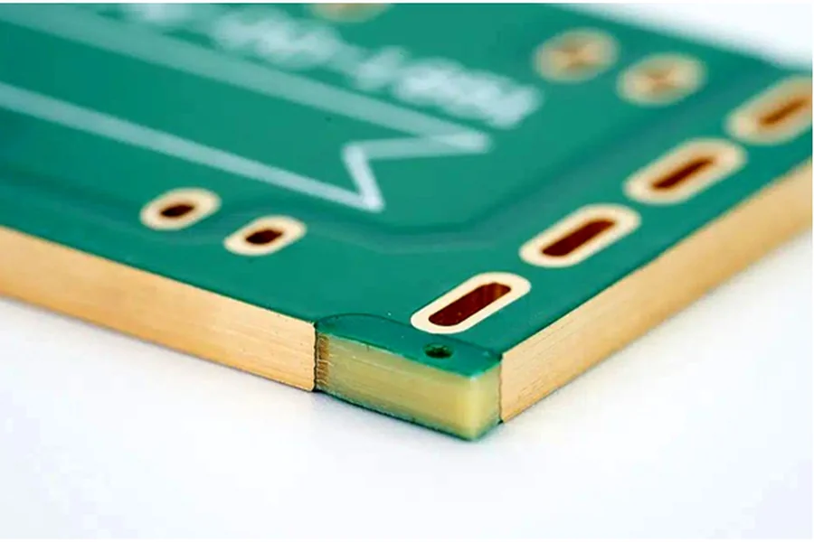
What Is a Heavy Copper PCB?
A heavy copper PCB is a specialized type of circuit board that features copper conductors with a thickness typically greater than 3 ounces per square foot (oz/ft²). Standard PCBs usually contain copper layers of 1 oz/ft² or less. In contrast, heavy copper boards may contain copper ranging from 3 oz/ft² to over 20 oz/ft², depending on the application requirements.
This increased copper thickness allows the PCB to carry higher currents and withstand greater mechanical stress, which is especially important for applications involving high power loads or temperature fluctuations.
Construction and Materials
The construction of heavy copper PCBs is more complex than traditional boards due to the thicker copper layers. These layers must be carefully laminated and plated during the manufacturing process to ensure uniformity and structural integrity.
Manufacturers use advanced plating and etching techniques to deposit the heavy copper onto the substrate. Techniques like differential etching and step plating are commonly used to ensure consistent trace widths and clean edges. The choice of base materials also plays a critical role; high-performance FR-4, polyimide, and ceramic materials are often selected for their thermal and mechanical properties.
These PCBs can also be designed as single-sided, double-sided, or multilayer configurations depending on the application’s complexity.
Key Benefits of Heavy Copper PCBs
The most notable advantage of heavy copper PCBs is their ability to handle significantly higher current levels without overheating or degrading. This makes them ideal for applications where energy efficiency and durability are critical.
Thermal management is another major benefit. Heavy copper layers act as effective heat sinks, dissipating heat away from sensitive components and extending the lifespan of the device. This is especially important in power supplies, automotive controllers, and motor drivers.
Mechanical strength is also enhanced. Thicker copper traces and pads resist damage from thermal cycling and mechanical vibrations, making these PCBs suitable for rugged and high-impact environments.
Moreover, the use of heavy copper enables the integration of high-power and low-power circuits on the same board, reducing the need for multiple boards and connectors. This simplifies the design and improves overall system reliability.
Applications of Heavy Copper PCBs
Heavy copper PCBs are used in a wide variety of industries where high reliability, durability, and power handling are essential.
In the automotive sector, they are used in electric vehicle (EV) chargers, battery management systems (BMS), and motor control units, where high currents and thermal resilience are necessary for performance and safety.
In industrial applications, these PCBs are common in power distribution systems, control panels, and heavy machinery where ruggedness and high current tolerance are mandatory.
In the aerospace and defense industries, heavy copper boards are used in navigation systems, radar modules, and power converters that must endure extreme conditions without failure.
For renewable energy systems such as solar inverters and wind turbine controllers, heavy copper PCBs help manage high voltages and currents efficiently, ensuring energy is transmitted with minimal loss.
Even in medical electronics, particularly in surgical tools and diagnostic imaging systems, heavy copper PCBs are used to support high-reliability and temperature-sensitive applications.
Manufacturing Challenges
Manufacturing heavy copper PCBs involves precise control over etching and plating processes. Handling thick copper layers requires adjustments in trace width, spacing, and lamination techniques. If not done correctly, issues like over-etching or layer misalignment can compromise performance.
Moreover, thermal stress during the manufacturing process must be minimized to prevent warping or delamination. Therefore, manufacturers need specialized equipment and strict quality control measures to produce consistent and reliable heavy copper PCBs.
Given the complexity, it’s important to partner with an experienced and capable manufacturer who understands the technical requirements and can offer customized solutions based on specific application needs.
Conclusion
The demand for heavy copper PCBs continues to grow as industries push the boundaries of power, durability, and performance. Whether in high-current automotive systems, robust industrial controls, or energy-intensive aerospace technologies, these PCBs provide unmatched reliability and thermal efficiency.
Choosing the right manufacturing partner is vital to unlocking the full potential of heavy copper technology. If you’re seeking dependable and high-performance PCB solutions, Viasion stands out as a trusted PCB Manufacturer in China. With years of experience in heavy copper PCB fabrication and assembly, Viasion offers customized, cost-effective, and quality-assured boards that meet global standards and demanding industrial requirements.